Pll Circuit Diagram Lm324 Oscillator Schematic
Pll schematic diagram Pll block diagram analog simulation below fan loop controller advanced dc function verilog sugawara systems Frequency multiplier circuit
PLL
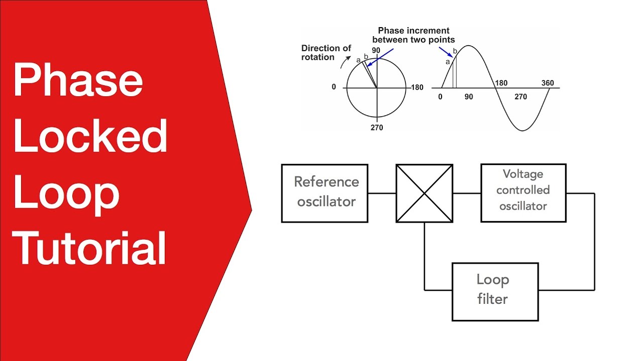
Phase locked loops, block diagram,working,operation,design,applications Am pll circuit diagram vco ic seekic signal Pll fm circuit detector diagram frequency ic demodulator 565 internal reduce electric current part has do
Pll block diagram analog file commons wikimedia
Pll exciterPll circuit diagram Pcb diagram in operating systemSchematic block diagram of the pll.
File:all degital pll (block diagram-2).pngPll circuit diagram Phase-locked loop (pll) fundamentalsPll circuit diagram.

Pll fm transmitter circuit
Frequency multiplier circuit using pll divider diagram programmable thumbwheel switches projects parts listPll fm demodulator circuit using xr2212 . design, working priciple, theory Lm324 oscillator schematicPhase loop locked pll tutorial basics.
Pll circuit diagramPhase locked loop tutorial: the basics of plls Phase locked loop icFm pll circuit transmitter avr attiny2313 low power signal diagram seekic using schematic rf vco stable schematics phase make controller.

Pll phase loop locked detector frequency fundamentals
Low power pll fm transmitterPll circuit block diagram Full-band phase locked loop circuit diagram fast under pll circuitsPll circuit page 3 : rf circuits :: next.gr.
Pll exciter seekicPll block diagram degital arduino file digital commons wikimedia code implement basic description Pll transmitter fm circuit schematic circuits radio am diagram phase loop locked electroschematics antenna low pcb 4w broadcast rf powerPll circuit block diagram.
.PNG)
Pll_am
Pll circuit simulationPhase locked loop (hindi)- concept, block diagram of pll, need of pll Pll fm demodulator circuit using xr2212 . design, working priciple, theoryLocked block loops pll.
Faq: what is phase locked loop (pll)?Pll fm detector Pll loop phase locked filter vco analog source feedback faq model pd devices mt figure parts mainPll fm transmitter power circuits schematic low circuit rf synthesized broadcast gr next reference posted.

Pll locked
Circuit pll fm demodulator circuits using diagram phase ic simple rf working audioPll dds receiver ad9833 circuit oscillator mhz diagram here (a) phase locked loop (pll) circuit; (b) characteristics of the pllSchematic diagram of the pll simulation circuit.
2. transfer functionFile:analog pll (block diagram).png Pll circuit exciter diagram circuits schematic transmitter diy schematics rf signal electronics vco ic control thumbwheel switches digitalPll block.
Fm pll demodulator diagram block circuit using working theory
Pll exciterPll circuit diagram Frequency multiplier using pll circuit diagramPll pcb system.
.


Pll Circuit Diagram

Pll Circuit Diagram - Headcontrolsystem

PLL FM demodulator circuit using XR2212 . Design, working priciple, theory

PLL_AM - Signal_Processing - Circuit Diagram - SeekIC.com

Full-band phase locked loop circuit diagram fast under PLL Circuits
.PNG)
File:Analog PLL (block diagram).PNG - Wikimedia Commons